Week 6 - PCB Design

For this week's lab, we used KiCad to design a simple printed circuit board (PCB) for an LED circuit. We started the lab by creating the schematic, and concluded by generating a 3D render and exporting the files necessary to produce the PCB.
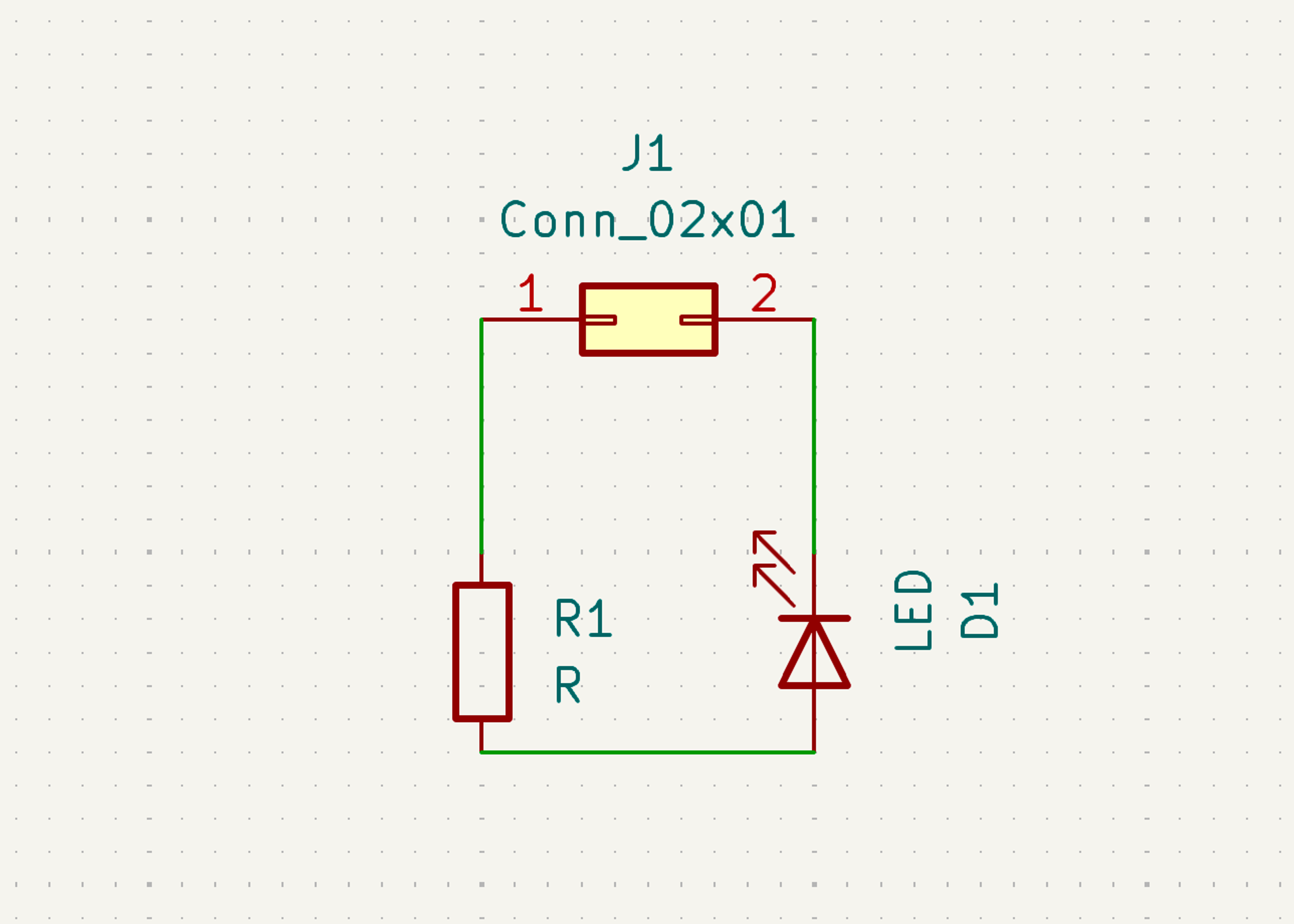
Schematic
The circuit consists of a JST connector (J1), resistor (R1), and LED (D1). We used this schematic to assign footprints to the components.
PCB Layout
Next, we used the PCB Editor to arrange the components on the board, create a board outline, and route the traces between components.

Before exporting our PCB, we checked for errors using the Design Rules Check (DRC).

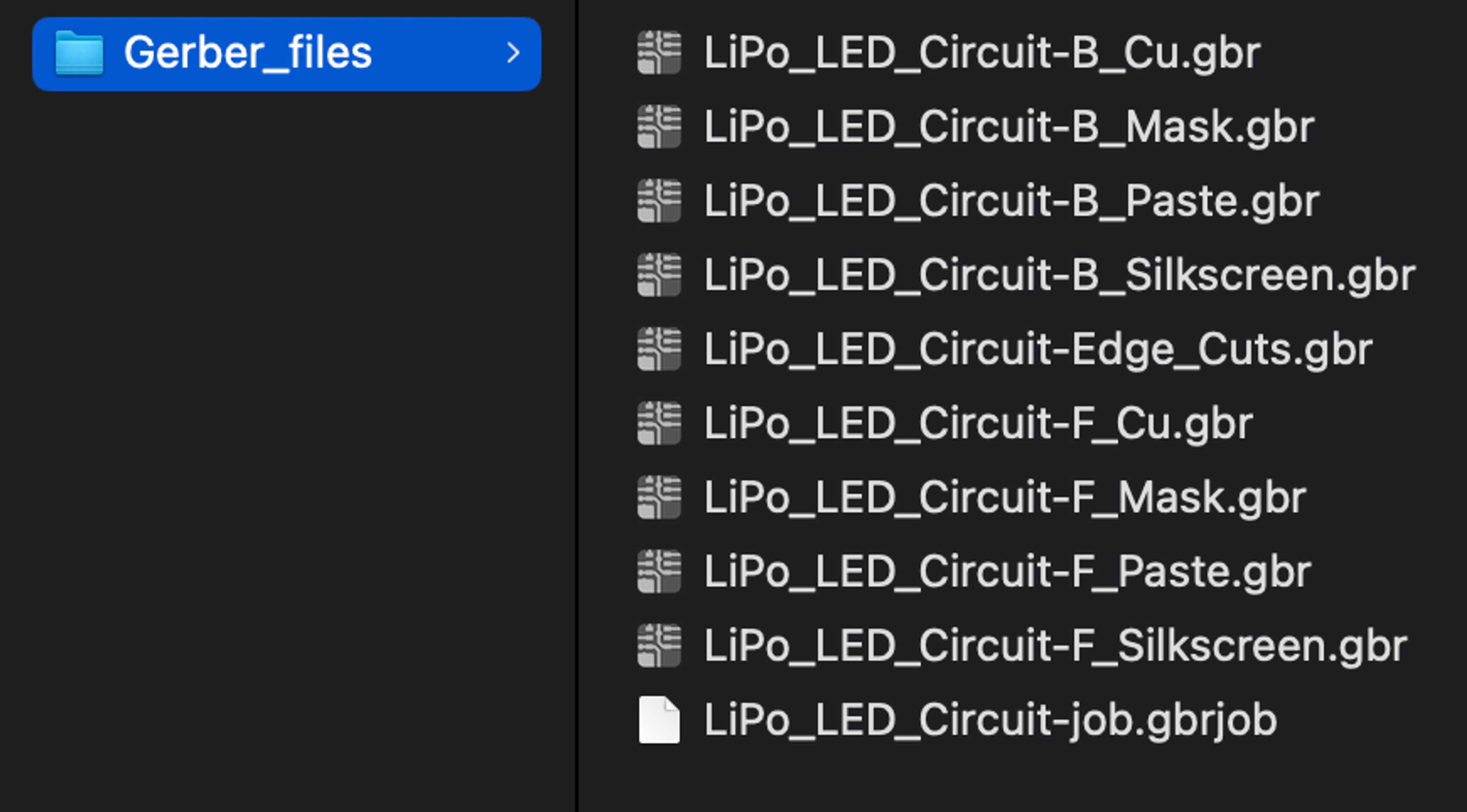
Finalized assets
We completed the project by exporting the Gerber files necessary for production. These files include the copper layers, drill files, edge cuts, and silkscreen layers necessary to manufacture the PCB.
3D Render
KiCad also includes a feature to display a nicely rendered 3D model of the PCB design. The results of my work are shown below.

File download
The files I created for this lab can be downloaded here.

